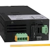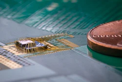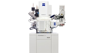
Zeiss introduces the Zeiss Crossbeam Laser, a new family of site-specific focused ion beam scanning electron microscope (FIB-SEM) solutions that accelerate package failure analysis and process optimization for advanced semiconductor packages.
Integrating a femtosecond laser for speed, a gallium ion (Ga+) beam for accuracy, and SEM for nanoscale-resolution imaging, the Zeiss Crossbeam Laser family provides package engineers and failure analysts with the fastest cross-section solution at the highest imaging performance, while providing minimal sample damage.
With its unique architecture, the Zeiss Crossbeam Laser family can rapidly cross section deeply buried package interconnects such as Cu-pillar solder bumps and through silicon vias (TSVs), as well as device back-end-of-line (BEOL) and front-end-of-line (FEOL) structures, in minutes instead of the hours or days of other approaches, all while minimizing artifacts and maintaining sample quality under vacuum.
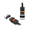
Besides failure analysis, the ZEISS Crossbeam Laser family enables structural analysis, construction analysis, reverse engineering, FIB tomography and transmission electron microscopy (TEM) sample preparation.
Features include:
- Femtosecond laser for large volume removal with minimal artifacts
- Gemini optics, which provide the highest image quality and analytics
- Ga+ FIB, which provides high-speed milling with 100nA combined with 500V fine polishing
- Accurate localized end pointing using FIB resolution
- Isolated laser chamber to segregate ablation contaminants from the main imaging chamber
- Easy sample transfers between the FIB-SEM and laser chambers without breaking vacuum
- Laser preparation suitable for many materials, including silicon carbide and glass
For more information, please visit: www.zeiss.com/pcs.