Micross Components, Inc. (“Micross”), a leading global provider of mission-critical microelectronic components and services for high-reliability aerospace, defense, space and industrial applications, expands its ASIC IP offerings with the addition of its next generation Nuclear Event Detector (NED), a replacement to the current 40-year old legacy NED products, which up until now were the only hi-performance NEDs available. These sensitive, high speed parts can be used to detect the initial rise of the gamma radiation pulse from a nuclear event and quickly shut down electronic systems for a brief interval in order to survive the blast and then resume normal operation. Applications include missiles, satellites, ground vehicles, or any system which needs to potentially survive a nuclear event. This new Nuclear Event Detector IC is manufactured on US soil in the Jazz Semiconductor Trusted Foundry, Inc. (JSTF), a wholly owned subsidiary of Tower Semiconductor NPB.
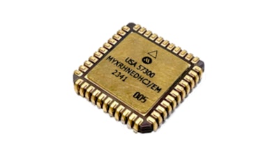
The Micross MYXRHNEDHCJ series Nuclear Event Detectors are available screened to Class H Military flow or Class K Space flow, and feature integrated differential drivers – providing improved overall noise immunity, 300% greater radiation dose sensitivity, and 25% faster response times in comparison with legacy devices. Legacy NED devices require external differential drivers, which typically increase weight due to additional radiation shielding requirements, and further increase response times by up to 100%. Customized NEDs can be optimized for the fastest response time, highest sensitivity, broadest dynamic range, reduced size and weight, or the most optimal combination of these features to address your specific requirements. A Micross applications engineering team is available to assist in this process.
The new Micross radiation hardened NED offers improvements in multiple areas, including:
- Reductions in size, weight and power (SWaP) due to the elimination of any shielding requirements on the peripheral circuitry, and lower power consumption
- 4X lower minimum dose rate threshold coupled with reduced dose rate threshold variation over temperature
- Increased noise immunity and sensitivity to nuclear events along with reduced delay time, resulting in 25% faster event detection
- A wide variety of packaging options
- Improvements in obsolescence mitigation and reliability, via a vertically integrated in-house sourced PIN diode and ASIC.
“Micross’ next-generation NED enables faster, more compact, and reliable nuclear event detection capabilities, with improved SWaP, performance and features, enabled through significant technology and design improvements applied to field proven building blocks,” stated John Santini, Chief Technology Officer, Micross Components. “These new NEDs provide greater safety and security in the protection of critical electronics subjected to a nuclear event, as they are able to recognize events with much greater sensitivity and react much faster to protect electronics than the current decades old NED devices.” A detailed data sheet is available for download from our NED page. Parts are currently in test. Engineering samples are available 4-6 weeks ARO.
For questions, please contact:
Christopher Stabile, Corporate Director of Marketing CommunicationsMicross Components, Inc.[email protected]