At every turn, demand for compute is rising across multiple fronts and all at once – AI, connectivity, cloud infrastructure, and electrification – with semiconductors as the common denominator. It’s unsurprising that the next era of these semiconductors is being shaped less by any single application than by the sheer scale of digital life, and the infrastructure needed to support it.
Humanity now generates vast volumes of data every single day, estimated at over 400 million terabytes, with this forecast to continue rising by around 20 percent over the next three to four years. Every message sent, algorithm trained, autonomous system deployed, and connected device monitored adds to a data ecosystem that must be stored, analyzed, and processed in real time. And behind every one of those processes lies a semiconductor chip, carrying ever-higher expectations for performance, power efficiency, and reliability.
 Investment in advanced processing solutions that ensure precise process control, traceability, and consistent repeatability across high-volume manufacturing environments is essential.Nordson
The Architectural Shift Reshaping the Industry
Meeting this demand for computing power is forcing a rethink of chip architecture. For decades, progress was largely driven by advances within a predominantly two-dimensional approach. Today, the industry is moving toward architectures that deliver performance gains through new forms of integration.
Two-and-a-half-dimensional (2.5D) designs have already gained momentum as manufacturers find new ways to integrate greater capability into a single package.
At the same time, the industry is evolving toward three-dimensional (3D) architectures, in which more functionality is built into a smaller footprint by integrating devices into increasingly compact, layered structures.
This shift is one of the key reasons advanced packaging has become such a critical growth area. By enabling greater integration within the package, advanced packaging is helping the industry keep pushing performance forward, even as designs become more intricate and the need for precision in manufacturing and quality assurance intensifies. The trade-off is that these architectures introduce unprecedented complexity into the manufacturing process.
Advanced Packaging: Innovation Meets Complexity
Advanced packaging has become one of the fastest-growing segments of semiconductor manufacturing, with annual growth forecasts commonly cited in the 10-12 percent range. Unlike traditional monolithic chip designs, modern packages may incorporate multiple dies, stacked structures, fine-pitch interconnects, and highly intricate internal features. These elements need to align with micron-level precision and perform reliably under demanding thermal and electrical conditions. As a result, quality assurance has become both more difficult and more critical.
While much of the industry focus centers on inspection and metrology as the gatekeepers of quality, the reality is that yield and reliability are equally shaped by the upstream processes that define how advanced packages are built in the first place.
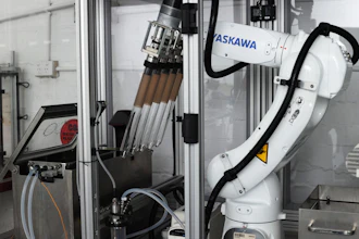
To manage this growing complexity, manufacturers are placing renewed emphasis on highly controlled processing solutions within the advanced packaging workflow. Precision dispensing technologies play a foundational role, enabling accurate application of underfill, encapsulation, edge bonding, and other materials that protect delicate interconnects, manage mechanical stress, and support long-term reliability. As interconnect pitches shrink and device architectures become more heterogeneous, consistency and repeatability at the micron level are no longer optional, they are prerequisites for yield.
Surface preparation and protection are equally critical. Plasma treatments are increasingly used to modify surface energy, improve adhesion, and ensure downstream materials perform as intended, particularly in tightly packed packages where uniformity is difficult to achieve through traditional means.
Conformal coating solutions add another layer of resilience, selectively shielding sensitive electronics from moisture, contamination, and harsh operating environments without compromising functionality. Meanwhile, selective soldering technologies enable precise, repeatable joints and electrical connections in complex assemblies, supporting both electrical performance and mechanical robustness. Together, these processing steps form a tightly integrated foundation for advanced packaging, enabling manufacturers to balance innovation with manufacturability.
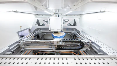
Building on this foundation, test and inspection add a critical layer of control and assurance across increasingly complex structures. Inspection technologies that once relied heavily on sampling or surface-level analysis, however, are no longer sufficient to ensure reliability in advanced packages. Instead, manufacturers increasingly require deep visibility into internal structures, micron-scale defect detection, and the ability to inspect complex assemblies at production-relevant throughput.
Technologies such as X-ray inspection, automated optical inspection (AOI), acoustic microscopy, and advanced metrology are increasingly essential tools for validating these intricate designs and protecting yield. They help manufacturers detect hidden issues that can compromise performance if left undetected, particularly as more critical structures are buried within the package, beyond the reach of surface inspection.
In this environment, inspection is evolving from a downstream checkpoint into an integral part of the manufacturing ecosystem – one that increasingly informs not only quality decisions, but process decisions too. This focus on yield becomes even more critical in an industry environment where semiconductor components can be subject to supply constraints, placing greater emphasis on minimizing waste and using them as efficiently as possible.
 Manufacturers increasingly require deep visibility into internal structures, defect detection at micron scale, and the ability to inspect complex assemblies at production-relevant throughput.Nordson
Artificial Intelligence Enters the Production Line
One of the defining and unavoidable manufacturing shifts of 2026, the impact of AI is no longer theoretical. It is showing up directly in production, not only driving demand for semiconductor chips, but reshaping how those chips are manufactured.
Traditional inspection systems relied on predefined rules or thresholds to identify defects. While effective in many scenarios, these methods can struggle as device complexity rises and variability increases across materials, structures, and designs. AI-driven inspection, by contrast, can learn from real production data to identify patterns and anomalies with greater consistency, helping reduce false calls while improving detection performance in challenging applications.
More importantly, AI shifts the role of inspection data. Instead of serving solely as a pass/fail gate, inspection increasingly acts as a feedback mechanism that informs process optimization, yield improvement, and maintenance strategies. In this sense, data, once treated as a byproduct of manufacturing, becomes a strategic asset. And as semiconductors move into more mission-critical systems, that capability becomes less of a ‘nice to have’ and more of a requirement.
The Electrification Effect
Nowhere is that pressure more visible than in electrification. Vehicles, for example, now contain dramatically more electronics than in previous decades, with semiconductors managing everything from battery control and power conversion to advanced driver assistance and connectivity.
 Vehicles now contain much more electronics than in previous decades, with semiconductors managing everything from battery control and power conversion to advanced driver assistance and connectivity.Nordson
In parallel, wearables, industrial automation systems, and smart consumer technologies continue to proliferate, each depending on increasingly sophisticated semiconductor components and tightening expectations around quality and traceability.
As electronics become more deeply embedded in daily life, the tolerance for failures continues to shrink. That places even greater emphasis on robust inspection, metrology, and process control across the semiconductor manufacturing ecosystem.
In this context, reliability is increasingly determined during the advanced packaging stage, where materials, processes, and design converge. Even minor variation in dispensing accuracy, surface condition, or interconnect formation can have outsized consequences once devices are deployed into safety-critical or always-on applications. As a result, manufacturers are investing in processing solutions that deliver precise control, traceability, and repeatability across high-volume production environments.
Reliable advanced packaging depends on tightly coupled process steps engineered not only for precision but also for long-term stability at scale. Controlled material deposition, consistent surface activation, and repeatable joining processes reduce variability and help ensure that devices leaving the factory will perform as expected throughout their operational life. As electronics move deeper into electrified vehicles, infrastructure, and connected systems, robust processing is no longer simply a manufacturing concern; it becomes a defining factor in product trust and brand reputation.
Inspection as an Enabler of the Next Semiconductor Era
Looking ahead, semiconductor growth will not be defined by design innovation alone. It will be shaped by the manufacturing capabilities that make complex architectures viable at scale – particularly advanced packaging, smarter quality assurance, and the ability to inspect and control processes with speed and precision.
Advanced packaging, AI-enabled manufacturing, and more automated factory environments are converging to redefine how semiconductors are produced. Inspection and metrology technologies sit at the center of that convergence, providing the visibility and confidence manufacturers need to manage complexity while maintaining yield, reliability, and efficiency.
For industry leaders, the takeaway is straightforward: the semiconductor growth story is far from complete. The forces driving demand – data growth, artificial intelligence, electrification, and connected devices – are still unfolding. At the same time, innovations in packaging and quality assurance are expanding what’s manufacturable, and therefore what’s possible.
 Srini Subramanian, Executive Vice President, Nordson Advanced Technology Solutions (ATS)Nordson
Srini Subramanian serves as executive vice president of Nordson Corporation’s Advanced Technology Solutions (ATS) segment, which delivers cutting-edge surface treatment, precisely controlled coating and dispensing and test and inspection solutions to support the electronics industry.