A practical method for mapping the flow of a current in devices with complex geometries that could be used to optimize circuit design has been developed at KAUST.
A traditional high-school physics experiment is to place iron filings on a piece of paper above a permanent magnet. The small metal particles will arrange themselves into a series of lines connecting the two ends, or poles, of the magnet. This enables students to visualize the otherwise invisible field lines that mediate magnetic attraction and repulsion.
Achieving this same type of map for the flow of an electrical current is particularly important in tiny electronic components. These components can have odd geometric arrangements, a result of the need for each element of the device to be packed into as small a space as possible. This means the current does not necessarily flow in a homogenous way.
Senfu Zhang and Xixiang Zhang, working with colleagues from KAUST, China and the United States, have now devised a method for visualizing the magnitude and direction of current flow through a magnetic thin film.
Several experimental methods have previously been developed to map current density in electronic materials. But these only do so indirectly, measuring stray fields rather than the currents themselves. Furthermore, they can be very expensive, or work only at very low temperatures. Computer simulations offer a cheaper alternative; however, they tend to oversimplify actual devices, ignoring nonuniformities or cracks in the material.
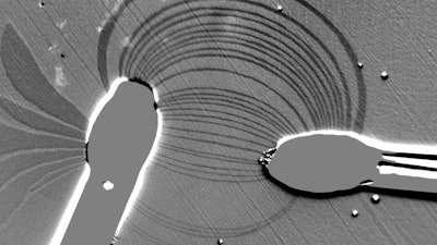
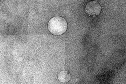
Instead, Zhang's team directly mapped the nonuniform electrical current distribution in layered platinum, cobalt and tantalum using the existence of so-called skyrmions. These "magnetic bubbles" can be imaged by a technique known as magneto-optical Kerr microscopy, which measures changes in the intensity and polarization of light reflected from a surface as a result of magnetic disturbances.
The skyrmions appear as round bubbles in the microscope images. "We found that when we passed a current through the material, only the front end of the bubbles moved forward, forming narrow, parallel strip domains," explains Senfu Zhang. The researchers showed that it was simple to extract the current flow from the growth direction of these patterns.
"This approach is not suitable for use in an actual device because it requires the deposition of Pt/Co/Ta on the device, but it is useful in the design phase," says Zhang. "Knowing the direction and magnitude of the electric current in each part of the device helps improve the design and performance."


